
Breakthroughs in Wafer Warpage Control During HBM Manufacturing
Wafer warpage has long been a critical yield and reliability concern in advanced semiconductor packaging, and it is especially consequential for High Bandwidth Memory (HBM). HBM’s stacked-die architecture, use of through-silicon vias (TSVs), and reliance on precise bonding and micro-bump formation all amplify the impact of any deviation from flatness. Recent breakthroughs in warpage control—spanning materials science, process engineering, metrology, and modeling—are improving yields, reducing costs, and enabling larger HBM stacks with higher interconnect densities.

Why wafer warpage matters for HBM
HBM stacks multiple DRAM dies and often interfaces with a logic die via an interposer or uses hybrid bonding. These processes require sub-micron planarity, accurate alignment, and controlled pressure during bonding. Warpage—out-of-plane deformation of wafers and thin dies—causes several problems:
- Alignment drift: Warpage during pick-and-place or bonding shifts die positions, resulting in misaligned micro-bumps or bonds and leading to electrical failures.
- Non-uniform bonding pressure: Variable flatness produces uneven contact, creating voids, weak joints, or over-compressed regions that reduce reliability.
- Thermo-mechanical stress: Warped stacks experience localized stresses during thermal cycling, accelerating delamination, crack propagation, and TSV failures.
- Manufacturing throughput hit: Wafers with excessive warpage often require rework, special handling, or are scrapped—reducing throughput and increasing cost per good unit.
For HBM, these issues translate directly into lower effective yields, higher test costs, and longer qualification cycles. Controlling warpage is therefore central to making HBM economically competitive.
Sources of warpage in HBM production

Warpage can arise at multiple points in the HBM value chain. Key contributors include:
- Thin-die effects: DRAM dies are thinned to tens of microns to enable stacking; thinner dies are more flexible and prone to bending under residual stresses.
- Die attach and underfill: Adhesives and underfills exhibit cure shrinkage and differing thermal expansion coefficients, creating stress gradients across the stack.
- TSV fabrication: TSV filling, liner deposition, and CMP (chemical mechanical planarization) introduce localized residual stresses.
- Interposer processing: Silicon or glass interposers undergo through-process thermal cycles and metal redistribution layer (RDL) formation that change mechanical properties and can induce bowing.
- Process-induced temperature gradients: Rapid thermal processes or uneven heating during bonding and reflow create differential expansion across wafers.
Materials advances that reduce intrinsic warpage
One major class of breakthroughs comes from materials innovation—both in the selection of materials and in their engineered behaviors.
- Low-stress dielectric films: New low-k and ultra-thin dielectric formulations with reduced intrinsic stress help minimize curvature introduced during deposition and curing.
- Adaptive adhesive chemistries: Novel adhesive systems that exhibit near-zero cure shrinkage or that relax internal stress post-cure help stabilize stacked structures.
- Compliant interposer materials: Use of glass interposers or engineered silicon-glass composites with tailored coefficients of thermal expansion (CTE) reduce mismatch-induced bending.
- Stress-absorbing encapsulants: Advanced encapsulants that redistribute and damp thermal and mechanical loads lower localized curvature during thermal cycling.
Process-level solutions and tooling innovations
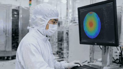
Process engineering improvements and specialized tools complement materials advances to control warpage during key manufacturing steps.
- Precision wafer thinning: Improvements in grinding and backside polishing produce more uniform thickness with tighter control over residual stress profiles, reducing post-thin curvature.
- Symmetric layer builds: Adjusting process flows to deposit or remove layers symmetrically reduces asymmetric stress and bowing—e.g., balanced RDL builds on both sides of a wafer when feasible.
- Low-temperature bonding and hybrid bonding: Lowering bonding temperatures reduces thermal excursions and CTE mismatch stress. Hybrid bonding techniques that combine direct oxide bonding with local metal connections minimize deformation compared with high-temperature reflow-only processes.
- Controlled cooling ramps: Optimized thermal ramp profiles during reflow and curing prevent thermal shock and reduce gradient-induced warpage.
- Active flatness tooling: Vacuum chucks, adaptive thinned-wafer carriers, and temporary stiffeners hold wafers flat during handling and processing steps, preventing deformation during placement and bonding.
Metrology and in-line monitoring advances
Better measurement and feedback systems are essential to both detect warpage early and enable closed-loop process control.
- High-resolution surface profilometry: Faster optical profilers and multi-point interferometry systems map wafer curvature at high throughput, enabling rapid binning and process adjustments.
- In-situ stress sensors: Embedded or temporary sensors that monitor stress evolution during curing and thermal cycles provide real-time feedback for adaptive process control.
- Machine-vision alignment correction: Advanced vision systems paired with adaptive placement algorithms compensate for measured bow during pick-and-place, reducing alignment errors at bonding.
- Data-driven process control: Analytics platforms correlate warpage signatures with upstream process parameters, enabling predictive maintenance and root-cause elimination.
Modeling, simulation, and digital twins
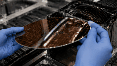
Simulation tools and digital twins are becoming essential for predicting and preventing warpage before wafers enter costly process steps.
- Multi-physics finite element models: Coupled thermo-mechanical-electrical simulations predict how TSVs, RDLs, adhesives, and thermal cycles interact to produce warpage across thousands of dies.
- Virtual process flows: Digital twins replicate entire packaging sequences—thinning, bonding, curing, reflow—so engineers can iterate on material choices and process parameters without physical prototypes.
- Yield-driven optimization: Simulation outputs feed optimization engines that balance yield, throughput, and reliability to identify Pareto-optimal process windows for minimum warpage.
- AI-assisted root-cause analysis: Machine learning models trained on historical process and metrology data identify subtle correlations that human engineers might miss, accelerating corrective actions.
Integration of these breakthroughs in production
Several leading OSATs and IDM (integrated device manufacturers) have begun integrating these advances into production lines. The effects are measurable:
- Yield improvements: Facilities report lower discard rates and fewer rework cycles, especially for multi-die HBM stacks exceeding four dies where warpage used to be a dominant failure mode.
- Higher stack heights: With improved warpage control, vendors can reliably build taller stacks (more dies) and push interconnect densities without proportional yield loss.
- Shorter qualification cycles: Better predictability and earlier detection reduce the number of qualification iterations required by customers, accelerating time-to-market for HBM-enabled devices.
- Lower total cost: Reduced scrap, fewer rework steps, and higher throughput lower cost-per-good-unit, improving economic viability for wider HBM adoption.
Supply-chain and business impacts
Technical breakthroughs reverberate through the supply chain and business models.
- OSAT differentiation: Service providers that master warpage control gain competitive advantage, attracting high-value HBM customers and commanding premium pricing for guaranteed yields.
- Material supplier opportunities: Demand grows for specialized low-stress materials, adaptive adhesives, and advanced thermal interface materials, creating new markets for chemical suppliers.
- Shift in qualification dynamics: Faster and more predictable qualifications reduce inventory buffers and shorten procurement cycles for system vendors.
- Capital allocation: With warpage risk reduced, customers may be more willing to commit to higher-volume HBM programs, encouraging suppliers to expand capacity and invest in next-generation packaging.
Remaining challenges and research directions
Despite progress, several hard problems remain. Addressing them will further unlock HBM scaling and cost reduction.
- Extreme thinness: As die thickness approaches single-digit microns for future nodes, mechanical fragility and out-of-plane deformation become harder to control without new carrier and handling solutions.
- Heterogeneous stacks: Combining dies with different materials (e.g., logic, analog, memory, photonics) increases complexity in CTE matching and stress management.
- Scaling to larger wafer sizes: Moving to larger wafers or panels (if adopted) will change warpage dynamics and require re-optimization of tooling and process flows.
- Cost vs. performance trade-offs: Some warpage-mitigation techniques add cost; the industry must balance the incremental process expense against yield gains and customer willingness to pay.
- Standardization of metrology: Diverse measurement approaches create inconsistent warpage specifications across supply chain partners; industry-wide metrics would improve interoperability and reduce qualification friction.
Future scenarios enabled by robust warpage control
Controlling warpage more effectively opens new design and market possibilities for HBM and advanced packaging.
- Taller HBM stacks: Reliable manufacture of deeper stacks enables higher capacity-bandwidth products for training-scale AI and HPC workloads.
- Heterogeneous integration at scale: Better warpage control makes integrating non-memory dies with HBM stacks feasible, enabling tightly coupled compute-memory modules.
- Panel-level processing: If panel-scale packaging becomes viable, precise warpage control will be a prerequisite for cost-effective mass production of stacked packages.
- Advanced thermal architectures: With warped-related yield risk reduced, designers can focus on thermal solutions that optimize performance without over-engineering for warpage contingencies.
Practical recommendations for manufacturers
Manufacturers aiming to reduce warpage-related losses should consider a coordinated approach that combines materials, process, metrology, and modeling:
- Adopt low-stress materials early: Evaluate adhesives, underfills, and dielectrics for intrinsic stress behavior and cure shrinkage as part of process selection.
- Invest in in-line metrology: High-throughput profilometers and stress sensors enable early detection and corrective action before costly downstream steps.
- Leverage digital twins: Use simulation-driven process development to reduce physical iterations and accelerate stable process windows.
- Collaborate with OSATs and material suppliers: Co-development shortens qualification and produces more integrated solutions tailored to specific stack geometries.
- Standardize warpage specs with customers: Agree on measurables and acceptance thresholds to reduce rework and speed qualification cycles.
Conclusion
Wafer warpage control was once a constraining factor for HBM scaling and cost-effectiveness. Recent breakthroughs across materials, tooling, metrology, and simulation are changing that narrative. By reducing intrinsic stresses, improving handling during critical steps, and providing real-time feedback coupled with predictive models, manufacturers can build taller stacks, improve yields, and accelerate qualification. These advances enhance the economic case for HBM across more market segments and enable more ambitious heterogeneous integrations.
However, the work is not finished. As die thicknesses shrink, stack complexity grows, and production volumes expand, manufacturers must continue to innovate and coordinate across the ecosystem. The next frontier includes handling extreme thinness, standardizing metrology, and developing cost-effective carrier technologies that keep fragile dies flat until they are permanently bonded. Successfully addressing these challenges will determine whether HBM can scale to meet future compute demands at sustainable cost.





